
Ashing in Semiconductor Processing
1. Principle of Ashing
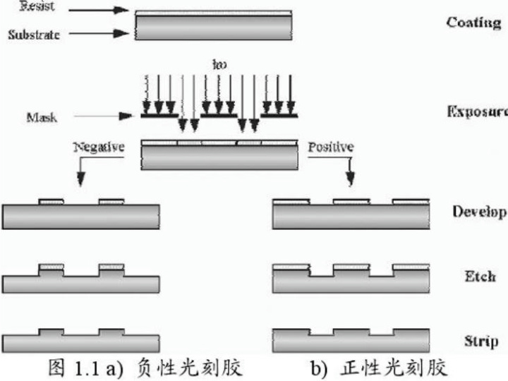
Ashing is a plasma-based photoresist removal dry process. After photolithography and etching, residual photoresist remains on the wafer and must be removed to prevent contamination of subsequent process steps.
2. Common Process Gases
| Gas | Chemical Formula | Function |
|---|---|---|
| Oxygen | O₂ | Most commonly used; oxidizes organic photoresist into gaseous products |
| Ozone | O₃ | Stronger oxidizing action; suitable for low-temperature processing |
| Trifluoromethane | CHF₃ | Controls selectivity; may form a polymer layer that assists or suppresses reactions |
| Argon | Ar | Provides plasma energy and physical bombardment |
| Nitrogen | N₂ | Controls the reaction atmosphere and limits excessive oxidation |
| Hydrogen | H₂ | Sometimes used to adjust reaction rate and selectivity |
⚗️ 3. Typical Chemical Reactions
Typical oxygen-plasma (O₂ plasma) ashing reactions are as follows:
Oxidation:
Oxygen radicals oxidize organic photoresist components (hydrocarbon polymers) into volatile gases:
CxHy + O* → CO↑ + CO₂↑ + H₂O↑
With fluorinated gases such as CHF₃:
CFx radicals form and modify surface reactions. They may also deposit a polymer layer that suppresses reactions or protects selected areas.
⚠️ 4. Process Considerations
Photoresist type, including positive, negative, or thick resist, affects ashing efficiency.
Excessive ashing may damage underlying films, such as low-k materials or oxide layers.
Power, pressure, gas ratios, and other process parameters require careful control.