
Read a Thermal Gap Pad Datasheet by Pairing Thickness with k-Value
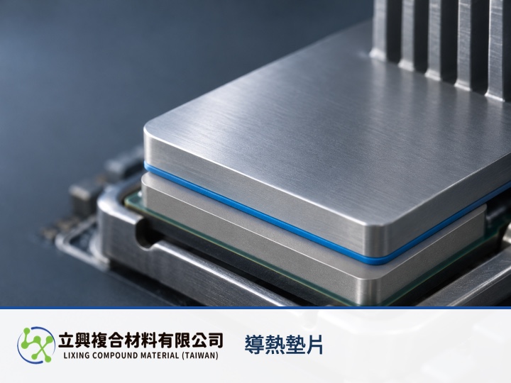
A thermal gap pad helps a CPU, GPU, or power module move heat into a cooling module by filling an uneven interface with a soft sheet. Pairing thickness with conductivity prevents a high datasheet k-value from hiding the resistance added by a longer heat path. Lixing thermal gap pads span 1.0 to 10.0 W/m·K and 0.25 mm to 1.3 mm, giving computing and power-electronics engineers a practical range for samples based on real gaps, pressure, and heat load.
Conductivity matters only when thickness is comparable
The Lixing thermal gap pad range covers conductivity grades from 1.0 to 10.0 W/m·K. A fair datasheet comparison still needs the same thickness and test conditions. When thickness changes, conductivity alone does not describe the material resistance in the heat path.
Soft grades help the pad conform to the interface
The published hardness range is 5 to 40 Shore B, and the official page describes low-pressure gap filling and conformity to uneven surfaces. That combination suits CPU, GPU, power-supply, and thermal-module interfaces. Actual contact resistance still depends on surface roughness, compression, and assembly pressure.
Thickness and format can follow the assembly space
Available thicknesses run from 0.25 mm to 1.3 mm, with die-cut parts or roll supply based on drawings. Color, size, shape, and surface tack can also be adjusted. Engineers can start with the tolerance-adjusted gap, then compare conductivity grades within the acceptable pressure window so the pad is neither unnecessarily thick nor too thin to maintain contact.
Equation: bulk resistance depends on more than k-value
NIST gives the one-dimensional steady-state slab relationship R = L / λ. R is area-normalized material thermal resistance in m²·K/W, L is thickness in m, and λ is thermal conductivity in W/(m·K). At the same conductivity, greater thickness raises bulk resistance; at the same thickness, greater conductivity lowers it. The relationship applies to a homogeneous flat slab at steady state with heat flow approximately normal to the specimen. It excludes both interface resistances, compressed thickness, surface roughness, and assembly pressure, so it is not a measured product total resistance. See the NIST thermal transmission reference.
Put datasheet values back into the real interface
For CPU or GPU cooling, record the source-to-sink gap, tolerance, allowable assembly pressure, contact area, and heat load before requesting samples. The thermal gap pad interface contact article covers the contact question, while this article stays focused on conductivity, thickness, and bulk resistance. This division keeps each page tied to one engineering decision.
Conclusion
Computing and power-electronics heat paths need both gap control and resistance control. The 5 to 40 Shore B range, multiple conductivity grades, and thickness choices let engineers request samples around actual assembly conditions. Share the gap, tolerance, contact dimensions, assembly pressure, and operating temperature with Lixing so the sample conditions match the design more closely.